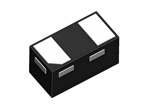
Failure to pass ESD tests even after adding ESD diodes is mostly not caused by defective components, but improper device selection or PCB layout. Based on our rectification experience, the main root causes are listed below:
First, excessively high clamping voltage (VC). This is the most‑frequent failure cause. Once the ESD diode turns on, it clamps voltage to a fixed level. If such clamping voltage exceeds the maximum withstand voltage of the protected IC, the chip will still be broken down. Always refer to the datasheet of the core IC during component selection and make sure VC is well below the chip’s voltage‑withstand limit.
Second, mismatched reverse working voltage (VRWM). If the selected VRWM is lower than the actual circuit operating voltage, the diode will stay near conduction threshold under normal operation, generating excessive leakage current or even false triggering. For instance, VRWM shall be 5 V or higher for 5 V signal lines.
Third, overlooked junction capacitance. ESD diodes with excessive junction capacitance applied on high‑speed interfaces (USB 3.0, HDMI, MIPI, etc.) will bring severe signal attenuation and sharply increase bit‑error rate. Capacitance below 5 pF is generally acceptable for USB 2.0, while USB 3.0 and HDMI require capacitance under 1 pF.
Fourth, unreasonable PCB layout, which is easily overlooked by many engineers. ESD diodes must be placed right next to connectors, with trace length preferably kept within 3 cm. Ground traces shall be short, straight and wide. Otherwise, parasitic inductance will push actual clamping voltage far above the rated value.
Therefore, merely mounting protective devices cannot guarantee test compliance. Both proper selection and layout are indispensable.
Jiangsu Daqi Semiconductor Technology Co., Ltd. © Copyright 2025
【Backstage】